The safety of your printed circuit board (PCB) is essential; however, not all boxes provide protection for this electronic assembly. It is important that an appropriate enclosure box provides protection for your electronics and allows them to function properly; manage their heat and give access to the components for maintenance. Iclosure has worked on a number of projects where a wrong choice of an enclosure box resulted in equipment overheating, malfunctioning due to incorrect interference from other surrounding equipment, and having difficulty maintaining the electronic assembly. All of these factors add up to a waste of your valuable time and money. Therefore, this guide provides you with information about the most important technical features of an enclosure box so that you will be able to choose the proper enclosure box for your upcoming electronics project. Some of the features covered in this presentation include; Standoff patterns, thermal management, etc.
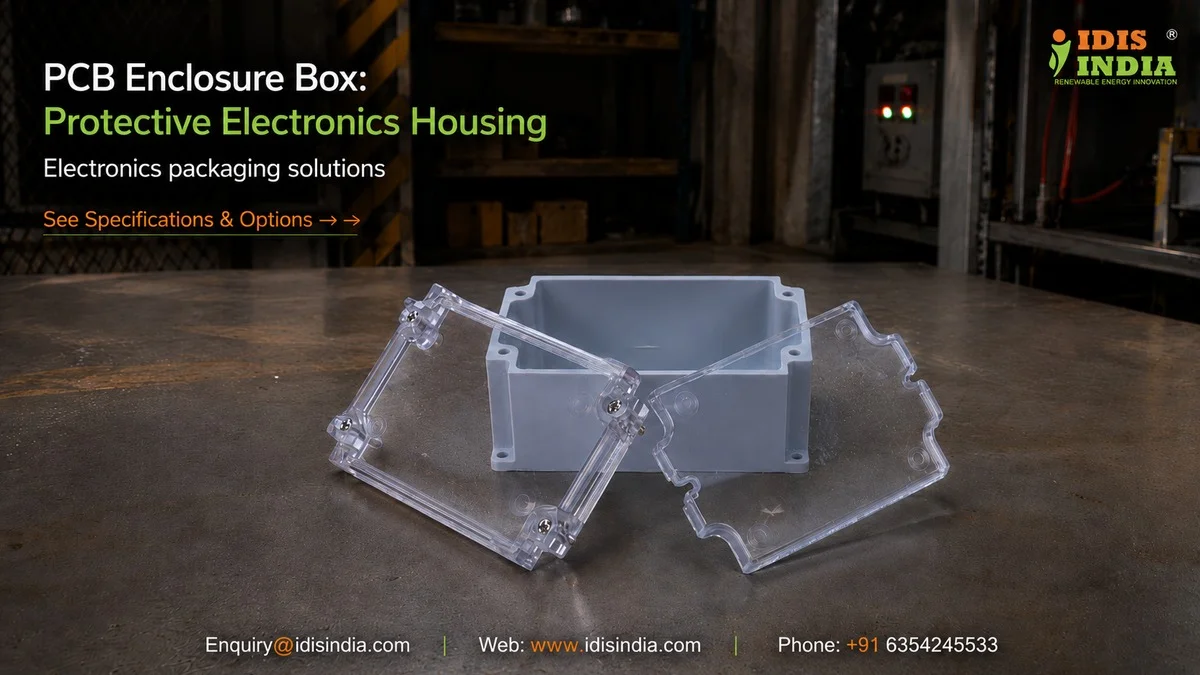
PCB Standoff Pattern Standards
Getting your PCB mounted properly starts with understanding how to come up with patterns for mounting standoffs. Most electronics engineers know this, but there are some details that you may not think about that may make a difference in your design. Standard mounting standoffs will be used based on industry standards, but your specific PCB may require you to create custom standoffs. Some common spacing that may be used would be a 0.1-inch grid on small PCBs to a larger grid for industrial applications. IDIS India manufactures enclosures with pre-drilled standoff holes; however, we also have blank enclosures available if you would like to drill your own holes. The material type you choose will make a difference as well; ABS would be easier to drill than Polycarbonate, but Polycarbonate is better quality for water and weather resistance. You should consider these factors when designing your mounting standoff pattern: the size and weight distribution of the PCB, component height variations on the PCB, any vibration specs related to the application, and whether there will be accessibility issues with regard to service or future debugging. One last note – when planning your mounting pattern, keep in mind that thermal expansion may affect mounting over time, so plan for some slight movement; this will be more pronounced in temperature-having cycle environments.
Component Clearance Height Planning
When assembling your enclosure for your PCB, make sure to reserve enough space in advance for any tall capacitors and for the amount of space where these parts will be installed or assembled. The best way to ensure you have adequate height clearance is by measuring your tallest components before assembled your enclosure. After measuring your tallest components, rotate the components to gain the maximum amount of height clearance possible. Be mindful of where you route wires and connector clearances, as that can affect the height made available for taller components as well. At I-closure, we have a selection of various depths in our enclosure line, so if you require an enclosure for a simple PCB, we have enclosures with shallow profiles, and for complex assemblies we have deeper enclosures to accommodate the necessary components. The dimensions of enclosures vary depending on which of our various enclosure models you choose, and the customizations that you require. Components that generate heat generally require additional height clearance provisions. When possible, locate these components away from the enclosure walls to allow for air circulation around them, or use enclosures with features for heat dissipation. In order to implement smart height clearance strategies, plan for: Space buffers for your tallest specified component(s), PCB deformation changes due to thermal shrinkage or warping when adding components, likely replacements or upgrades, variation of manufacturing tolerances between PCB’s and enclosures.
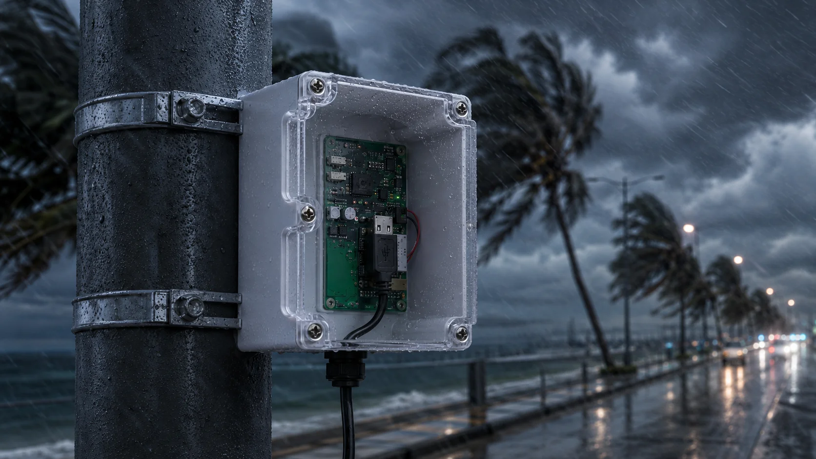
Ventilation Slot Positioning Methods
Heat generation by electronics is unavoidable; if you neglect the appropriate ventilation system, as such, heat becomes your greatest enemy. However, just creating holes is not going to provide you with a proper air movement strategy — means and methods of creating airflow must be an integral part of your ventilation design. The best way to achieve natural convection is by positioning intake slots low and exhaust slots high. This chimney effect will allow the movement of air through the enclosure, eliminating the need for fans or an external power supply.
The position of your intake and exhaust slots is influenced by both the layout of your PCB as well as its associated heat sources. In addition, you should place your intake slots away from any sensitive components that could be affected by either dust or moisture. Furthermore, if possible, you should always position your exhaust slots above any components that generate heat.
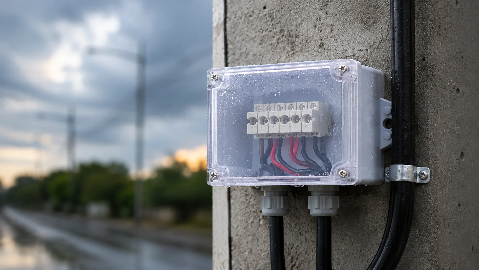
Keeping in mind that ventilation can affect your product’s IP rating, it is necessary to pay extra attention to your ventilation design in the IP65 and IP67 enclosure line for continuing to ensure the same level of protection of the enclosure. In some cases, you will also want to consider filtered vents or strategic slot placement to reduce the possibility of water ingress.
When designing your ventilation, keep the following strategies in mind:
– Use smaller multiple slots rather than fewer large slots
– Utilize angled slots to prevent direct entry of water
– Use mesh filters to protect against dust in industrial environments
– Strategically place ventilation slots within the enclosure so that structural integrity of the enclosure is not compromised
Airflow Pattern Optimization
Predictable airflow patterns can be achieved by utilizing proper ventilation techniques. Using physics to your advantage, hot air will inherently rise, so you want to use hot air’s tendency to rise in your design. To accomplish this, heat sources need to be mapped out first, so that airflow paths can be determined to move cool air near hot components while efficiently exhausting hot air. Avoid dead zones of stagnant air; always ensure there are adequate air circulation pathways throughout your system.
EMI Shielding PCB Integration
Due to the presence of electromagnetic interference, your product performance can suffer dramatically! While the enclosure contributes greatly towards EMI shield performance (provided that you have designed the integration correctly), conductive type enclosures will provide you with the optimal approach to achieve an EMI shield. Plastic type enclosures can also provide you with a useful approach to providing EMI shield protection, provided that you implement the correct techniques.
Do not forget to consider using conductive coatings, gaskets, and strategic grounding to help you attain your EMI shield goals. Additionally, the PCB-to-enclosure integration will have an impact on the performance of the EMI shield by establishing one of the main paths from the circuit ground to the enclosure ground that will create the EMI shield. Poor PCB-to-enclosure ground connections will create gaps in the ground path that allow EMI to pass freely through the gaps in the shield. IDIS India has various types of enclosures, including conductive coated enclosures; however the availability of these enclosures is subject to different requirements, so contact IDIS India for current availability and lead times.
When you are designing your EMI shield, consider the following key issues regarding EMI shielding performance: Continuous ground plane connection around perimeter of enclosure; Correct gasket selection for removable panels; Filtered cable entries to minimize conducted EMI; and The proper location of sensitive circuit components will help you to minimize EMI from other sources.
Ground Plane Connection Techniques
To ensure your PCB has a proper EMI Shield, connect the PCB ground plane to the enclosure form effectively. The quality of this connection can often be the determining factor in whether or not the product will pass EMC compliance tests. Using multiple connections offers a better result than single connections. Distributing these ground connections around the edge of your PCB creates a more effective shield for your application and provides extra redundancy in case of failure. There are many ways to make the ground connection(s) between the warhead and the enclosure depending upon the material from which they are made and their intended use. The use of conductive gaskets will produce a good connection between the two when they are to be taken apart at some point. The use of conductive adhesives or direct contact will create reliable connections when the two are to remain permanently together. The following are additional methods to connect your PCB to the enclosure (i.e. using spring contacts to connect the PCB to the enclosure that can accommodate thermal expansion, the use of conductive standoffs that create a mechanical connection between the PCB ground plane and the enclosure, dedicated ground straps or laces for applications where grounding is critical, and PCB Edge plating that creates a mechanical contact between the PCB edge and the enclosure wall). Ground loops may also be an issue. So, be sure to design your ground scheme to minimize the creation of multiple paths for current to flow that could cause ground bounce or interference.
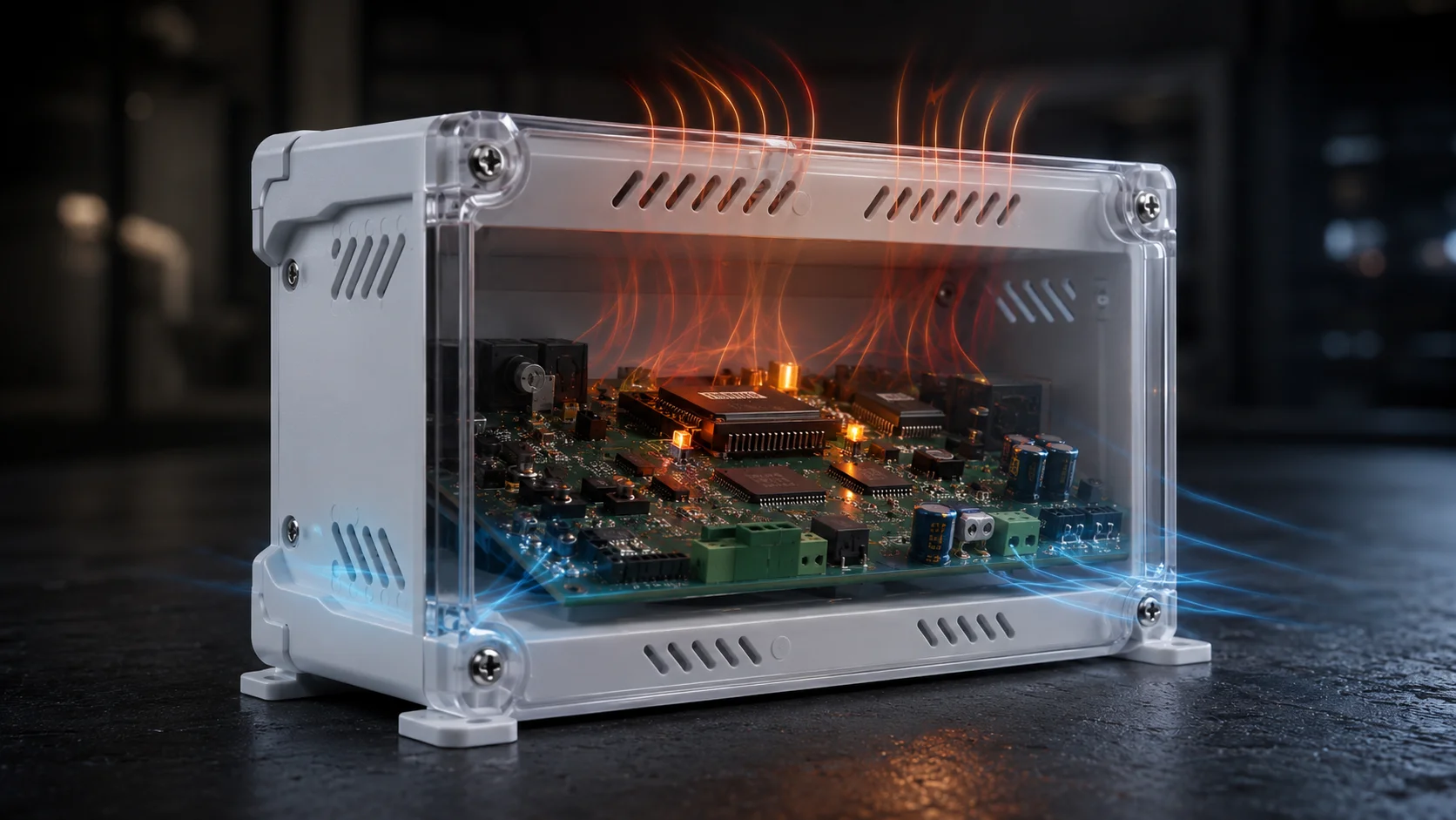
PCB Thermal Interface Design
Electronics are affected by heat. Thermal management has been considered as part of the enclosure design process from the beginning, not simply as an afterthought. Geometric interfaces provide for transferring heat from the hot component to either the walls of the electrical enclosure or heat sink. This geometry governing these interfaces has an effect on how reliable and how well the product performs. Direct contact is the most effective way to transfer heat from high power components. The heat-generating components must be mounted to the metal area of the enclosure or to dedicated heat sinks. The use of thermal interface materials improves the heat transfer between surfaces that are separated by a gap. Although, the thermal design of the enclosure includes more than thermal sinks. The thermal characteristics of the assembled enclosure are affected by the location of the components, the design of the airflow system, and material selection for the enclosure and the individual components. Mounting provisions for heat sinks and thermal management devices may be incorporated into an I-closure enclosure. Depending on your specific requirements and the environmental conditions, heating/cooling performance characteristics can differ.
Heat Sink Integration Options
Cooling devices outside the enclosure can provide excellent cooling, but they can cause issues with sealing the enclosure. Internal cooling devices maintain a high level of protection but may not be able to provide optimal cooling. Hybrid solutions that utilize both types of cooling are an option to provide cooling when necessary while providing flexibility and protection.
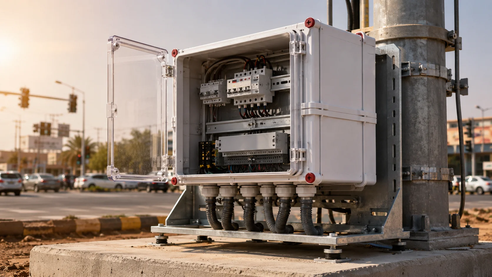
Electronic Assembly Access Panels
A PCB enclosure must allow for repair, programming and debugging access; however, if they are not designed correctly, these access points could compromise the security of the enclosure. During the testing and development stage, removable panels provide full access to the PCB while continuing to offer protection during normal use. Smaller access ports are used for specific access needs such as programming connectors or test points and can provide higher IP ratings than a removable panel. Many different factors will affect both the performance and protection level of a product based on how the access point is designed, including proper gasket design and proper latching systems to ensure a dependable seal. When creating access points, consider the type of tools that will be necessary to remove the panels; some applications may require quick access to the access points while other require more tamper resistant systems. Access point design considerations include: Panel Size versus level of protection Gasket compatibility to the environment in which the product will be used Latching type mechanisms appropriate for the application Cable management for removable connections Consider maintenance procedures; are technicians going to have to gain access to the product in the field? Design your access panels for the conditions under which they will be used instead of just for laboratory testing conditions.
Modular Access Solutions
Having several small access panels tends to work better than having just one big access panel; this way you can only access the area you require and not expose the entire PCB. Additionally, modular design is able to accommodate different access requirements; for example, programming ports may need to be accessed often whereas calibration points will only need to be accessed occasionally. Want to protect your PCB with the right enclosure? Contact IDIS India right now so that we can talk about your individual needs. We’ll help you pick out the best PCB enclosure box for your needs, paying close attention to all the technical features that will ensure great performance of your electronic devices!